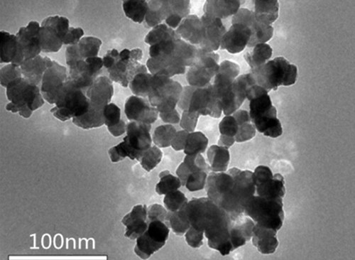
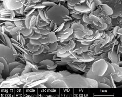
1. Classification of Scanning Electron Microscopes
Scanning electron microscopy can be divided into thermal electron emission type and field emission type according to the different ways of electron generation. The filament used for thermal electron emission type is mainly tungsten filament electron microscopy. Field emission type
The distinction between hot field emission and cold field emission.

2. Classification of Transmission Electron Microscopy
Transmission electron microscopy can be divided into thermal electron emission type and field emission type according to the different ways of electron generation. The filaments used for thermionic emission mainly include tungsten filaments and lanthanum hexaboride filaments. There are two types of field emission: thermal field emission and cold field emission.

3. The similarities and differences between scanning electron microscopy and transmission electron microscopy
The two have similar requirements for the sample: solid, as dry as possible, as free as possible from oil contamination, and the external dimensions meet the size requirements of the sample chamber.
The difference is:
(1) On sample preparation: The penetration ability of TEM electrons is very weak. Transmission electron microscopy often uses high-energy electron beams of several hundred kilovolts, but it still requires grinding or ion thinning of the sample or ultra-thin slicing to micro nano scale thickness, which is the most basic requirement. SEM hardly requires sample preparation and allows for direct observation. Most non-conductive materials require the production of conductive films (such as gold coating).
(2) On imaging: During SEM imaging, the electron beam does not penetrate the sample but scans its surface. During TEM imaging, the electron beam penetrates the sample. The spatial resolution of SEM is generally between XY-3-6nm,
The spatial resolution of TEM can generally reach 0.1-0.5nm.
4. What is the thickness requirement for the sample when conducting TEM testing?
The thickness of the TEM sample should preferably be less than 100nm. If it is too thick, the electron beam is not easily transmitted, resulting in unclear images and poor imaging.
5. What are the requirements for the sample when conducting TEM testing?
-The sample is generally required to be dry. If the sample is a solution, it needs to be dropped onto a certain substrate (such as glass), dried, and then sprayed with carbon. If the sample itself is conductive, there is no need to spray carbon.
6. How to perform TEM on nanoparticles in aqueous solution?
TEM samples must be tested under high vacuum conditions, while nanoparticles in aqueous solutions cannot be directly measured. Usually, micro grids or copper mesh are used to remove the sample and place it in a sample pre extractor. After drying, it can be placed in an electron microscope for testing. If the sample size is small and only a few nanometers, use a non porous carbon film to scoop up the sample.
7. Thickness requirements for high-resolution samples
When taking high-resolution TEM images, it is best to control the sample thickness below 20nm. Thinner samples can reduce electron beam scattering, thereby improving image resolution. For powders with a diameter less than 20nm, they can be directly removed and observed on carbon support films or small pore micro grids. If the particle diameter is greater than 20nm, it is best to embed it first, and then use ion thinning technology to thin the sample to a thickness suitable for observation.
8. How to make TEM for powdered samples?
The key to preparing powder samples is to have a good supporting film and disperse the powder evenly with moderate concentration. After the supporting membrane is completely dry, it should be placed into an electron microscope for observation to avoid rupture of the supporting membrane under electron beam irradiation.
① Pre attach a thin support film to the copper mesh;
② Select a reasonable dispersant based on the properties of the powder sample;
③ Disperse the powder evenly through ultrasound to form a suspension;
④ Place the powder solution on a copper mesh using drop or scoop methods and dry it;
⑤ Ensure that the powder sample is evenly distributed on the copper mesh and free of contaminants;
⑥ Gently blow the copper mesh with an ear wash ball to ensure that there is no easily falling powder.
9. Why spray gold on non-conductive or poorly conductive samples?
SEM imaging is the process of obtaining signals of secondary electrons and backscattered electrons through a detector. If the sample is non-conductive or has poor conductivity, it will cause the accumulation of excess electrons or free particles on the surface of the sample that cannot be guided away in a timely manner. After a certain degree, repeated charging and discharging phenomena will occur, ultimately affecting the transmission of electronic signals, causing image distortion, deformation, shaking, and other phenomena. After gold spraying, the conductivity of the sample surface will be enhanced, thereby avoiding the phenomenon of accumulation.
10. Does spraying gold affect the morphology of the sample?
After spraying gold on the surface of the sample, only a few to a dozen layers of gold atoms are covered on its surface, with a thickness of only a few nanometers to a dozen nanometers, which has almost no effect on the morphology.
11. How to demagnetize magnetic powder?
Magnetic powders can be prepared using Zeiss field emission electron microscopy without demagnetization, following the preparation of conventional powder samples. If some block shaped strong magnetic materials can be demagnetized by heating or applying an external magnetic field, there are specialized demagnetizers in the market.
12. Why are magnetic particles generally not allowed to undergo transmission electron microscopy?
Because the sample needs to be dropped onto a dedicated support film when making magnetic materials, the magnetic material may be attracted to the lens, affecting TEM resolution and contaminating the electron microscope.
13. Why do different instruments produce different effects on the same sample?
If the camera parameters are set similarly, the effect will not be significantly different. Only different instruments have different parameter settings (probe, voltage, beam current, etc.) during shooting, and the specific impact of which parameters needs to be analyzed based on the shooting results.
14. What are the specific application scenarios for spraying gold, platinum, and carbon?
Metal targets such as Au and Pt can increase conductivity, increase the generation of secondary electrons and backscattered electrons, have good signal-to-noise ratio, and reduce electron beam penetration, with the aim of obtaining high-quality images. C target material, suitable for analysis of EDS, EBSD, WDS and other components.
15. When taking SEM photos. Why spray gold or carbon on non-conductive or poorly conductive samples?
When observed with a scanning electron microscope, when the incident electron beam hits the sample, charge accumulation occurs on the surface of the sample, forming charging and discharging effects that affect the observation and photographic recording of the image. Therefore, before observation, conductive treatment should be carried out, such as spraying gold or carbon, to make the surface of the sample conductive.
16. The sample does not contain carbon element, but the result shows a content higher than 70%, which deviates too much from the actual situation. How to handle it?
The energy spectrum is insensitive to elements with atomic numbers less than 11, and errors in carbon, nitrogen, and oxygen are common. In addition, carbon pollution comes from a wide range of sources, such as conductive adhesives, contact between samples and hands, DP pumps, air dust, and so on. Special attention should be paid to the unsuitability of light elements such as carbon, nitrogen, and oxygen for energy spectrum analysis. In addition, if Mapping testing is required, there may be obvious carbon, nitrogen, and oxygen in the background other than the sample, which may not be distinguishable from the sample, Mapping pays special attention to light elements such as carbon, nitrogen, and oxygen. If the content is higher than the actual value, it can be artificially reduced.
17. The reason for the unclear results of the morphology shooting
The poor conductivity of the sample leads to unclear shooting results; The shooting requirements are too high, and the instrument itself cannot meet them; Focusing or astigmatism is not adjusted properly, which is generally rare; It is also related to device configuration and installation environment.
18. In the SEM images of some samples, obvious electron beam black spots can be seen. How to remove the electron beam spots in the interface?
Electron beam black spots may indicate that the sample is relatively dirty and has accumulated carbon. It is recommended to pay attention to the storage environment or conduct timely testing on the prepared sample.
19. What is the reason for the ethanol dispersion sample taking morphology, which shows a layer of film on the substrate?
The reason for the appearance resembling a film is due to the dispersion of ethanol followed by gold spraying.
20. Why does transmission electron microscopy have no color?
Color is determined by the color of light, that is, the frequency of electromagnetic waves, and the light of an electron microscope is not natural light, but an electron beam light source, so it cannot display colorful colors. Transmission electron microscopy can reveal fine structures smaller than 0.2um that cannot be clearly seen under an optical microscope, which are called submicroscopic structures or ultrafine structures. To see these structures clearly, it is necessary to choose a light source with a shorter wavelength to improve the resolution of the microscope. In 1932, Ruska invented the transmission electron microscope with an electron beam as the light source. The wavelength of the electron beam is much shorter than that of visible light and ultraviolet light, and the wave of the electron beam is
The length is inversely proportional to the square root of the voltage of the emitted electron beam, which means that the higher the voltage, the shorter the wavelength. At present, the resolution of TEM can reach 0.2nm, and the images obtained by electron microscopy are "grayscale images" that reflect the number of electrons (i.e. brightness), without color information.
SAT NANO is a best supplier of alloy powder, metal powder, oxide powder, carbide powder in China, we are not only supply the products, but also we can supply SEM and TEM and other technical service, if you have any enquiry, please feel free to contact us at sales03@satnano.com


